

| Ultraviolet and Visible Devices Based on III-Nitride Semiconductors
High Quality Superlattices for Effective P-Type DopingEffective p-type doping of wide bandgap III-nitride semiconductors is difficult due to the high activation energy of most acceptors. This problem is more pronounced for AlGaN compounds with increasing Al content. 
Calculation of the sheet carrier density in AlGaN/GaN superlattices. Through theoretical modeling and material growth optimization, researchers at CQD have successfully demonstrated the highest p-type conductivity conductivity ever reported for AlGaN. The technique made use of AlGaN based superlattices, based on a patent awarded in 1997 to Northwestern University ("III-Nitride superlattice structure, The method of increasing acceptor level and decreasing contact resistance," US patent, 5831277, March 19, 1997). These superlattices exhibited a very high free hole concentration of 4.2x1018 cm-3 and a very low resistivity of 0.19 Ω.cm. 
Atomic scale TEM of the very well ordered AlN/sapphire substrate interface. N-type doping also poses a significant challenge for high Al content AlGaN layers. By careful optimization of the SiH4 flow, and the use of a high-quality AlGaN/AlN superlattice template on AlN buffer we were able to realize Al0.5Ga0.5N:Si with n ~1x1018 cm-3 and μ~40 cm²/V·s. The addition of indium yields a carrier concentration of n~5x1018 cm-3 and mobility of μ~80 cm²/V·s. World's First Lateral Epitaxial Overgrowth of GaN on SiliconBecause of the lack of commercially available native substrates, obtaining low defect III-Nitride semiconductors has remained one of the most challenging issues in this area for numerous years. The dislocations that are formed when growing III-Nitrides heteroepitaxially, i.e. on non-native substrates, have proved detrimental not only to the material's structural, optical, and electrical quality, but also to the device performance. 
Crossesction of lateral epitaxial overgrowth on silicon. Researchers at CQD have successfully and extensively explored innovative approaches to reduce the dislocation density in GaN by several orders of magnitude through the use of lateral epitaxial overgrowth (LEO). In particular, researchers at CQD were the first to demonstrate the LEO of GaN on silicon substrates. World's First Solar Blind Ultraviolet Photodetectors and Focal Plane ArraysThe Center for Quantum Devices (CQD) has demonstrated many record-breaking achievements in the development of UV, visible -blind and solar-blind photodetectors. Photodetectors are devices that transform electromagnetic radiation (light) into an electrical signal (current or voltage). Several applications demand that these devices detect specific energies of light while ignoring others, e.g. sensitive to UV and not visible or infrared light. Using III-Nitride technology, inexpensive, efficient, highly sensitive and robust devices can be achieved. 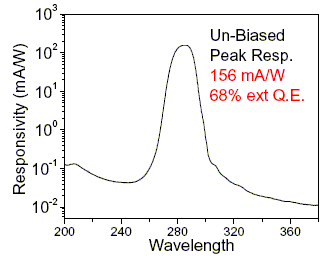
Highest efficiency response of back-side illuminated solar-blind photodiodes. These high efficiency Al-GaN based UV photodetectors can be used in a number of military and civilian applications including early missile threat warning, secure space-to-space communications, chemical and biological agent detection, engine/flame detection, furnace monitoring, UV dosimetry, ozone/pollution monitoring, and UV astronomy. Numerous types of photodetectors have been investigated at CQD, including photoconductors, Metal-Schottky-Metal detectors, Schottky photodiodes, pin photodiodes, and most recently avalanche photodiodes. 
Spectral response from AlGaN p-i-n photodiodes. Using high quality AlInGaN compound semiconductors grown via metalorganic chemical vapor deposition, high quality visible-blind and solar-blind photodetectors have been demonstrated exhibiting record high efficiency, visible- or solar-blindness, excellent sensitivity and unparalleled versatility. The CQD is the only research group to have demonstrated the entire range of AlGaN photodetectors, which exhibit a cutoff wavelength from 225 to 365 nm and thus can be tailored to any specific application. 
Solar blind UV image from a AlGaN focal plane array. In an effort to push the technology toward focal plane arrays, both front- and back-illuminated AlGaN pin photodiodes have been realized with record solar-blindness and record high efficiency. These photodetectors have been fabricated into 320 x 256 focal plane arrays and hybridized to commercial readout integrated circuits. This has lead to the realization of a working solar-blind focal Plane array camera. World's First Back Illuminated Avalanche Photodiodes and Geiger-Mode Single photon DetectorsResearch into avalanche photodiodes (APDs) is motivated by the need for high sensitivity ultraviolet detectors in numerous civilian and military applications. By utilizing low-noise impact ionization based gain, GaN APDs can deliver gains of more than 10000 in linear mode; and operating in Geiger mode, the gain can exceed 1×10⁷ and thus single photon detection becomes possible. We have experimentally studied impact ionization in GaN and found that the hole ionization coefficient is significantly larger than that for electrons. This means that back-illuminated devices exhibit larger gains; we have also observed excess multiplication noise factors that are more than three orders of magnitude lower. 
Comparison of photocurrent and excess multiplication noise of the same detector under either front- or back-illumination. By using high-quality delta-doped p-GaN a consistently lower breakdown voltage can be realized, without significantly affecting the dark current. This has allowed a more than 50x improvement in the maximum gain realized, as compared to devices grown with traditional bulk p-GaN. In addition to controlling the material and doping quality it is also possible to carefully design the structure to minimize the external bias necessary to reach the critical electric field necessary for breakdown (typically of 3 ×10⁶ V×cm-1). This can be accomplished by reducing the width of the combination absorption/multiplication layer in a traditional p-i-n device structure; however this also increases the leakage current of the diodes, and thus, the dark count rate in Geiger mode. To help overcome this, we have developed a separate absorption and multiplication APD structure (SAM-APD). By separating the absorption and multiplication regions using a p-i-n-i-n structure it becomes possible to absorb more than 99% of the light in the bottom layers resulting in nearly pure hole-injection into the multiplication region. This maximizes the advantage of the higher hole-ionization coefficient resulting in a device with a maximum linear mode gain of more than 40,000. 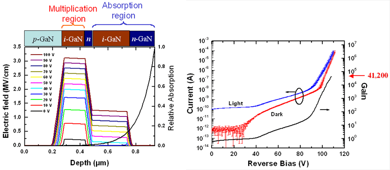
SAM-APD device structure showing optical absorption in the bottom layers for pure hole injection in the high-field gain region resulting in significantly improved avalanche multiplication. We have realized the world’s first back-illuminated GaN APDs operating in Geiger-mode, and thus capable of single photon counting. These Geiger-mode APDs operate using gated pulsed-quenching to detect very low UV-light levels. The spectral response shows a flat Geiger-mode response for photon energies above the bandgap, and a high visible-light rejection ratio. The single photon detection efficiency of these devices is more than 23%, with dark count rates of less than 10 KHz. 
Single photon detection efficency (SPDE) and dark count rate (DCR) of various size Geiger mode APDs. Violet, Blue, Green Light Emitting Diodes and LasersThe Center for Quantum Devices has developed the III-Nitride material growth and processing of visible Light Emitting Diodes LED) and lasers. Light-Emitting DiodesUsing InxGa1-xN/GaN double hterostructures and multiquantum well structures, researchers at the Center have demonstrated high-brightness blue and green LEDs.   LEDs are important optoelectronic devices because they are compact light sources which are more efficient, more reliable, consume less energy and last longer than conventional incandescent light bulbs. Blue, green and white LEDs can be made using III-Nitride semiconductors, as developed at the Center. III-Nitride LEDs are beginning to replace light bulbs in traffic signaling and to be used in bright outdoor full color displays in addition to many other applications such as indicator lamps, automobile lighting, and outdoor and indoor LasersHigh-performance laser diodes fabricated from III-nitride materials are complex, yet highly attractive devices due to their potential use in a number of applic ations. The Center for Quantum Devices has been pursuing the MOCVD growth and development of these devices, which incorporate InxGa1-xN/GaN multi-quantum wells. To achieve high efficiency lasers, the CQD has been investigating lateral epitaxial overgrowth (LEO) as a means to improve III-Nitride materials by reducing defects during the growth on both sapphire and silicon substrates. 
Electroluminescence photograph and spectrum of one of CQD's visible LEDs. Semiconductor lasers are highly efficient, compact devices that emit an intense, coherent, monochromatic beam of light. Blue laser diodes stand to satisfy a number of application needs including high-density data storage, high capacity DVD, high resolution color printing, and laser displays. 
Photo-, electro-luminescence and stimulated emission from CQD's laser structure. Ultraviolet LEDs at 340, 280, 265 and 250 nmResearchers at the Center for Quantum Devices are developing ultraviolet LEDs based on wide bandgap AlInGaN semiconductor materials, for use in chemical and biological agent detection systems, water purification and air sterilization. 
Typical UV LED structure (left) and electroluminescence spectra from a range of UV LEDs with emission peaks between 340 and 247 nm (right) . Thanks to extensive research work on the material growth and device structure, including the material optimization described earlier, researchers at CQD have successfully demonstrated AlIn-GaN based ultraviolet LEDs emitting at 340 nm, and for the first time in the world, at wavelengths as short as 280 and 265 nm, in addition to wavelengths as short as ~250 nm. Researchers at CQD have also demonstrated the ability to grow high power UV LEDs by choosing native substrates (GaN). The 340 nm UV LEDs grown on GaN substrate showed an order of magnitude improvement in the light output of the devices compared to the devices grown on sapphire. 
Output power from a range of UV LEDs with emission peaks between 280~250 nm. For the short wavelength of 280 nm, output powers as high as 6.5 mW from AlGaN-based single quantum well ultraviolet light emitting diodes were demonstrated. The output power in continuouswave mode reaches a value of 310 μW. For the shorter wavelength of 265 nm, output powers as high as 5.3 mW from AlGaN-based single quantum well ultraviolet LEDs were demonstrated. The output power in continuous-wave mode reaches a value of 170 μW. For devices with very short emission wavelengths ~250 nm, output powers as high as 3.2 mW under pulse operation. Quantum Dots and NanostructuresThe Center for Quantum Devices is also conducting research work on quantum dots and nanostructures in III-Nitride semiconductor materials. When used in the active regions of light emitters, such structures are expected to enhance their luminescence properties.  Both self-assembly of dots and direct writing/patterning through electron beam lithography and dry etching have been investigated. Also GaN nanowires based on the Vapor-Liquid-Solid growth mode have been realized. The picture above shows an SEM image of GaN nanowires with an average diameter of 30 nm. Last Updated 10/08/2008 |
| © 2020 Center for Quantum Devices, Northwestern University Disclaimer |
 Channel